Retrocomputing Asked by da66en on August 25, 2021
I was interested in a recent interview of Masayuki Uemura, one of the engineers who designed the Nintendo Famicom in the early 80s. During initial design phase of the Famicom, one of the first things he says he did was reverse engineer the video game consoles of the time. This quote from him of this interview caught my interest:
I had a semiconductor manufacturer dissolve the plastic covering on
the chips to expose the wiring underneath. I took pictures, blew them
up, and looked at the circuitry to understand it.
Exactly what process is he talking about? At a time when ICs were of low complexity (compared today), could you actually see each transistor on the silicon and reverse engineer it?
As voltage shows up on electron microscopes, somewhat, but you cannot see hidden layers. ICs are getting more 3d.
Answered by David Pickett on August 25, 2021
An engineer who worked at National Semiconductor back when reverse engineering was legal described a conference room wall covered with a patchwork of photos representing an entire Intel microprocessor. They visually extracted the circuit from the image.
Answered by John McGehee on August 25, 2021
This was part of how AMD developed their first 80386.
AMD had long been a second source for Intel x86 chips. Originally the agreement was that Intel would provide details to AMD, who would build their own chips. As time went on Intel wanted to end this agreement or at least prevent AMD from making use of it. This led to numerous court battles.
AMD expected to win, so one of their approaches was to reverse engineer Intel's chips by doing what you describe-- decapping them, and working out the designs by direct examination under microscopes. They took lots of pictures. Eventually AMD won out and they were able to produce the Am386. I believe AMD used other approaches in parallel, but I don't know details of them.
[My only source is my memories from working at AMD at the time. I wasn't on this team but the story was well known around the company.]
Answered by Tom Harrington on August 25, 2021
From the '80s, chips increasingly used standard cell components. So if you can recognise a standard cell, you don't need to recognise each transistor in it. Companies like Phillips and ES2 provided standard cell libraries.
Built in self test became popular at that time. It's a technique for piping a known state into and out of the chip, running it for some cycles, then reading the result. It's used to check if a chip works after making the wafer but before packaging it. It could also be used to reverse engineer the chip.
To replicate a chip, you'd also need to replicate any firmware. Compaq's reverse engineering of the IBM PC's code to evade copyright is a important setp the IBM PC story: https://en.wikipedia.org/wiki/IBM_PC_compatible
Answered by Michael Grazebrook on August 25, 2021
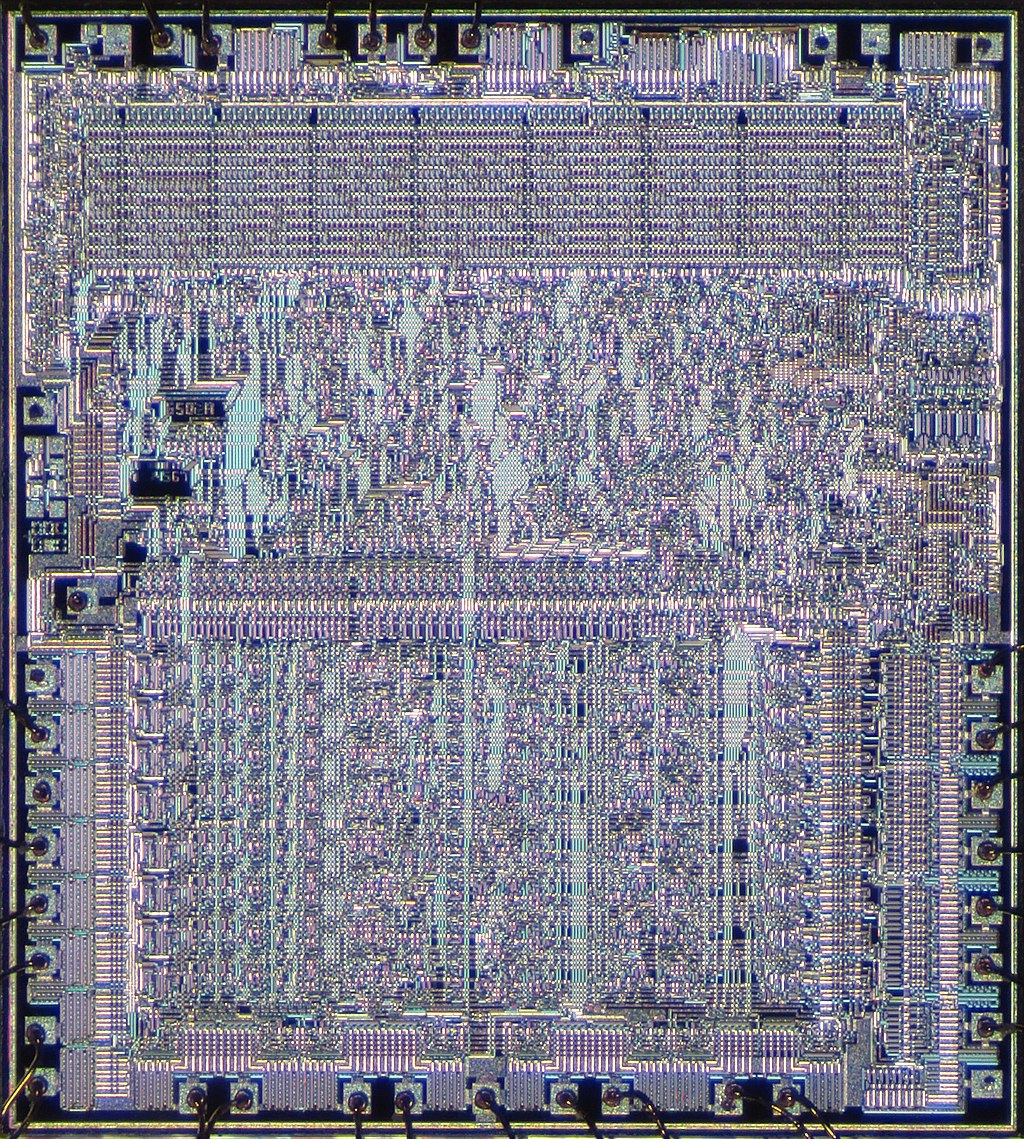
It's worth noting what you can see, and what you can't.
First, you cannot see any feature that is much smaller than the wavelength of light that you are using. In 1995 I designed a chip for my Master's thesis in 1.2um technology; features are clearly visible under microscope. Features in 0.5um technology might be visible, but by 1997 0.25um technology was the big thing, and individual transistors would not be visible. Today, reverse engineers pretty much have to use electron microscopes - optical microscopes are useless.
Second, you can see only those features that have some physical significance: you can see metal layers, polysilicon (the material used to make transistor gates), the contacts and vias between these layers, as well as the "thinox" demarcating a transistor, which is really a slope between a thick layer of silicon dioxide and the thinner layer used to make a transisitor gate.
You cannot see doping - what makes an NMOS device different from a PMOS device, so you cannot tell which is which just by looking. You can infer which is which using the circuit connectivity, if you know what you are looking for. Similarly, for NMOS devices, you cannot distinguish enhancement mode devices from depletion mode devices by looks alone.
Answered by d3jones on August 25, 2021
Yes, reverse engineering of chips with a conventional optical microscope in the late 1970s and early 1980s is generally possible.
Although of course, there are limitations. Firstly, the number of wiring layers is important - already two layers of metallization and two layers of polysilicon make reverse circuit design much more difficult. Secondly, chip traps specially created by developers to prevent copying - this, in particular, was practiced by Zilog with the Z80. Thirdly, the size of the circuit / number of transistors, taking into account the amount of labor and available auxiliary techniques - already Motorola chips of level 68000 were a very expensive task.
However, in the game consoles of those years, only the second version of the problems was relevant.
Answered by Wheelmagister on August 25, 2021
(More of a memory dump related to Stephen's answer)
At a time when ICs were of low complexity (compared today), could you actually see each transistor on the silicon and reverse engineer it?
Yes.
Just try it yourself. Take some 1980s TTL, like a 7400 - I'm sure you find some on old boards - and crack it open. Usually it separates well from the plastic. Put it below a children's microscope and you will see the structure for each of the four gates. With some basic knowledge about semiconductors, you'll be able to draw the schematics free hand.
It's what I did to my first pocket calculator at the age of 13. Of course, I didn't have the knowledge to really turn what I saw (it was a calculator chip, not just a 7400) into a useful drawing, but I still remember my father's face, showing a mixture of being mad and amazed at the same time, when I showed him the drawings and he realized that I utterly destroyed the calculator he has spend ~50 Mark (*1) on a few days before. Essentially it foreshadowed my future of taking everything apart :))
Slicing up a 1976-1980 8-bit CPU is not really challenging. Structure sizes were about 5-10 µm, so not even a microscope was needed. A good camera with a decent lens and average film will do it.
Let's take for example the well-known 6502. It was manufactured in an 8 µm process with a chip area of roughly 4x4 mm. The needed film quality is defined by 'lines' - that is, pairs of consecutive lines that still can be distinguished. 8 µm wide details on a 4000 µm means we need at least 2000 lines over the width of the photograph taken. With 35 mm film, this means 2000/35 = ~60 lines/mm. An average ASA 100 colour film will deliver anywhere between 60 to 150 lines/mm.
So even the cheapest hobby film could be used in reverse-engineering a 6502. This is especially true as we talk analogue film, so no pixel artefacts (*2). Of course, this is the upper limit to start, still making it hard to decide some structures. So more lines are better. B&W films of similar (low) quality and price deliver 300-500 lines/mm, while good go past 1000. More than enough to give a crisp clear view of every detail (*3).
Bottom line: in 1980, a consumer class camera with a good lens and cheap film was all that was needed to dissect any CPU at the time ... well, yes, and a lot of time at hand to understand what was shown :))
In fact, one can still do so with the latest chips except the problem is that nowadays, a picture, even a very good one, wouldn't do it alone. The 6502 had 5 layers and basically all of them can be identified right away. Nowadays chips are made of more than a dozen layers, many of them connective ones, covering the underlying transistors a great deal. Today it needs careful scraping of of layers to get a look inside, much like archaeologists digging out a settlement. But still doable, as now fine tools like lasers can be used to peel each layer. Heck, there is even a guy in Berlin(?) doing this for fun with today's chips, like Apple's latest ARM cores.
*1 - 50 Mark in 1974 may equal about 100 Euros nowadays. Doesn't sound much, but it was quite a lot money to us (you know, ye goode olde time when we had no shoes and had to walk to school in snow and rain, uphill in both direction). Back then, filling a large car (Mercedes) was less than 20 Mark.
*2 - To be correct, analogue film also shows granulation, as the photo sensitive area is made up of discrete particles. But unlike a CCD they are randomly placed, resulting in kind of a ... well ... analogue resolution. Important for this task is that due to the random placement none of the usual digital artefacts will be created. The picture will simply start to blur.
*3 - Superior material can deliver up to 10,000 lines. That's enough to cover any modern CPU with a single shot. Of course, at that point optics does start working a bit differently, but that's another story.
Answered by Raffzahn on August 25, 2021
With a powerful enough microscope, you can see each transistor. Reverse-engineering silicon then boils down to carefully removing each layer (ceramic or plastic to expose the chip, then each metal layer), taking detailed photographs, and figuring out what each part does. For CPUs of the era, this was already possible in the early eighties.
Ken Shiriff does this nowadays on older chips; he just posted a detailed example of this process on the Intel 8086. Michael Steil famously reverse-engineered the 6502 nearly ten years ago, and gave a great presentation on the topic at CCC.
Answered by Stephen Kitt on August 25, 2021
Get help from others!
Recent Answers
Recent Questions
© 2024 TransWikia.com. All rights reserved. Sites we Love: PCI Database, UKBizDB, Menu Kuliner, Sharing RPP